The envisioned industrial TOPCon process route includes process steps that can be fully/partially transferred from state-of-the-art PERC batteries, including several additional process steps required to improve conversion efficiency. It is widely believed that the technological maturity and proven industrial readiness of the process technologies used in PERC have facilitated the transition of the photovoltaic industry towards more efficient battery concepts such as TOPCon. Another potential advantage of adopting this progressive approach is that as long as there is sufficient area in the PERC facility, the existing PERCon production line can be upgraded for TOPCon processing, increasing the minimum number of process steps.
The formation of tunnel oxides and the deposition of intrinsic/doped polycrystalline silicon are two key processing steps beyond the current PERC process, which mainly determine the TOPCon processing process route. The characteristics of these layers are crucial for designing subsequent battery processing steps, aiming to achieve high open circuit voltage (V overclocking) and the low series resistance promised by the TOPCon concept. In addition to these steps, industrial TOPCon batteries are mainly based on more expensive n-type substrates and require integrated boron emitter diffusion processes, which have lower industrial maturity compared to the phosphorus diffusion processes commonly used in p-PERC batteries.
Low pressure chemical vapor deposition (LPCVD) of amorphous layers after in-situ growth of thermal tunnel oxides is currently a production ready technology for industrial processing of TOPCon batteries. Meanwhile, the TOPCon process route based on alternative amorphous silicon deposition technology is currently being studied in facilities and is expected to be ready for mainstream production in the near future. In fact, the photovoltaic industry is currently considering various process routes and a wide range of technological options for the TOPCon concept, both in terms of technical feasibility and economic feasibility. However, the mass production of these TOPCon Concept car and the economic competitiveness of the current mainstream PERC batteries are still an unresolved issue. According to reports, the current PERC concept has a mature process sequence in large-scale production, with an average conversion efficiency of up to 23%. The continuous improvement in cost-effectiveness to date has made PERC the preferred choice for large-scale installation in public utilities. Therefore, the additional capital and operating costs required to establish and operate TOPCon manufacturing facilities need to be offset by improvements in battery/module/system level conversion efficiency, in order to further reduce the Levelized Power Cost (LCOE) in large-scale photovoltaic installations. In-depth research on the cost-effective manufacturing options of TOPCon is highly relevant to the photovoltaic industry. The photovoltaic industry is currently researching different options for transferring the TOPCon concept from laboratory research to production lines, as a potential opportunity for the next evolutionary solar cell technology upgrade to PERC.
In this work, our goal is to use bottom-up total cost of ownership (TCO) calculations for various process steps and related battery processing routes in the photovoltaic value chain to develop a cost driven strategy for large-scale manufacturing of TOPCon based solar cells. Based on existing literature, industry feedback, and the technological development of Fraunhofer ISE, we first discuss the industrial process route based on LPCVD for the TOPCon concept. Then, we outlined and discussed the status of various alternative technologies. Based on the results of production preparation, we conducted cost of ownership (COO) calculations for different amorphous silicon (a-Si) deposition technologies, with the aim of identifying and outlining technically feasible process routes for industrial TOPCon solar cell architecture, and analyzing its competitiveness with mainstream double-sided PERC batteries in terms of battery/component/system costs, as well as the levelized cost of electricity (LCOE) for utility scale green space installation. Finally, sensitivity analysis is conducted on the selected TOPCon route to determine the minimum increment required for PERC conversion efficiency to achieve economic competitiveness. Based on our findings, we will discuss current and future technological choices for the large-scale production of TOPCon solar cells.
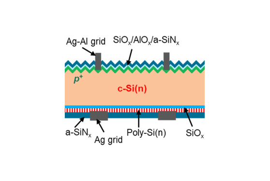
We focus on the TOPCon architecture, using screen printed contacts on both sides of the n-type silicon substrate, as they have the potential to achieve the highest conversion efficiency compared to the double-sided p-PERC concept and have the best mass production prospects. The unit structure studied is shown in Figure 1. TOPCon solar cells are based on n-type c-Si substrates with boron (p) emitters on the textured (front) side. The front is passivated by a dielectric stack of passivation and anti reflection layers. The back of the textured/semi polished or polished surface has tunnel oxides and doped polycrystalline silicon layers as passive carrier selective contacts, and is hydrogenated with amorphous hydrogenated silicon nitride (a-SiN) stacked+x) layers as a hydrogenation source to passivate the suspended bond 2 interface in Si-SiO. Metallization is achieved by screen printing the silver or silver aluminum mesh at the front and screen printing the silver mesh at the back, considering double-sided applications. The reference PERC battery is a p-type double-sided solar cell with a phosphorus (n) emitter, front and rear passivation layers, and double-sided screen printed contacts. Each section of this article outlines the detailed process route for the studied cell types. The bottom-up total cost of ownership (TCO) calculation is carried out along the photovoltaic value chain using the "SCost" model developed internally by Fraunhofer ISE. This model calculates the cost of ownership (COO) of each manufacturing process step in the photovoltaic value chain based on SEMI standards E35 and E10, and constructs a process route at the factory level that considers equipment interdependence, indirect production costs, and capital costs to estimate the total cost of ownership of the required solar cell architecture. Determine and compare different commercially feasible amorphous silicon deposition technologies based on equipment and process parameters, which are based on data provided by industrial equipment manufacturers and our own industrial equipment process parameters within the PV-TEC test line of Fraunhofer ISE. For each deposition technology, determine the most promising process route for mass production based on the technical and economic feasibility of the adopted process steps. The following are the main selection criteria set for the optimal manufacturing solution: a) availability of industrial tools, b) process compatibility, c) availability of all process parameters required for COO modeling, d) lean processes, and e) successful demonstration of process functionality. Perform a sensitivity analysis of the levelized kilowatt hour cost to determine the minimum gain of conversion efficiency required for the TOPCon concept, in order to maintain competitiveness with the double-sided p-PERC benchmark at the levelized kilowatt hour cost level.
So far, industrial screen printed TOPCon solar cells on n-type substrates are based on LPCVD a-Si/poly Si deposition technology. Usually, a primarily amorphous silicon layer is deposited first, followed by a high-temperature annealing step to form a polycrystalline silicon (poly Si) layer with a mixture of amorphous and crystalline phases.
LPCVD is used as one of the important processes established in semiconductor facilities for depositing highly conformal a-Si/poly-Si layers under low pressure conditions. The main advantages of this technology are: a) good thickness distribution along the wafer and boat, b) a pinhole free layer with good step coverage, c) maintaining the previously formed impurity distribution in the wafer due to the relatively low deposition temperature close to 600 ° C, d) a large number of wafers in each batch, and e) selecting in-situ doping with a constant doping curve.
For the TOPCon concept studied in this work, it is necessary to deposit a phosphorus doped a-Si/poly Si layer (a-Si (n)/poly Si (n)) on the back of the solar cell. Here, silane (SiH4) is used as a precursor for silicon deposition, and diluted PH3 (2 in N) can be optionally used to add dopants to the layer. The performance of the layer is influenced by deposition pressure, silane concentration, and dopant content, with the most significant being the deposition temperature. Under the same process conditions, the addition of doped gas will significantly affect the growth of thin films, i.e. the silicon deposition rate. For example, according to process conditions, including PH3, it has been reported that flux can reduce the deposition rate several times, and an increase in pH value further exacerbates the deposition rate 3 flux. This led to two methods of LPCVD a-Si deposition - a) deposition of the inherent a-Si/poly Si layer, followed by the formation of a poly Si (n) layer through non in-situ POCl3 tube diffusion process, b) deposition of in-situ doped a-Si (n)/poly Si (n) layer, and subsequent thermal annealing in N. In Figure 2, we calculated the COO of the intrinsic layer and phosphorus doped layer with the same thickness of 150 nm, considering that the deposition rate of the in-situ doped growth layer is about 36% lower than that of the intrinsic layer. LPCVD deposition is carried out here in a frontal configuration, where two facing wafers are placed in one slot.
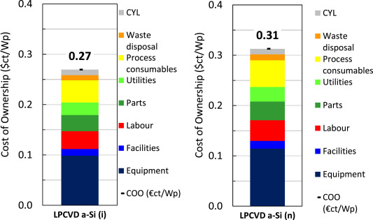
Figure 3 schematically shows the TOPCon process route based on LPCVD a-Si technology, as well as the reference process route for double-sided p-PERC. For p-type PERC batteries (double-sided p-PERC), alkaline textured wafers receive phosphorus emitter 3 through POCl based on a low-pressure tube diffusion furnace. Afterwards, a laser source was used to selectively form a high phosphorus doped region on the front, aiming to drive phosphorus atoms from the phosphorus silicate glass (PSG) layer to the silicon substrate. This selective emitter method is mainly aimed at reducing the recombination of a few charge carriers below the metal contact. Next is the post emitter removal or chemical edge isolation (CEI) process. PSG etching and ozone based cleaning are in the same Wet chemistry online tool. Ozone cleans the surface of silicon oxide and then removes the oxide by final HF immersion before the surface passivation step. By growing about 2nm of thin thermal silicon oxide before back passivation (PECVD AlO), advanced passivation x/a SiNx stacks for the front and back sides and front (PECVD a-SiNx) are envisioned, which is considered a necessary step to achieve a high average conversion efficiency of 23.0% in double-sided p-PERC production. After the passivation process, screen printing is performed on the back by printing the Ag contact pad first, followed by printing the Al mesh, and then printing the Ag mesh on the front. After rapid firing (FFO), a regeneration process is required to compensate for the loss of conversion efficiency caused by photo induced degradation (LID), which is related to the formation of boron oxygen complexes.
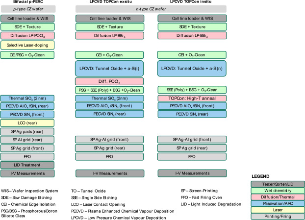
The main difference between the two TOPCon routes is the method used to form doped a-Si/poly Si layers. After the texture processing process, boron doped 3 precursor was used to form a boron (P) emitter in a tube diffusion furnace for TOPCon batteries using BBr. Next is the online Wet chemistry process, which removes the rear emitter on one side while keeping the BSG layer on the front intact; Before executing an ozone based cleaning sequence. The BSG remains intact on the front to protect the boron emitter from etching during the single sided etching (SSE) process of polycrystalline silicon. Afterwards, tunnel oxides are formed in situ by oxidizing the c-Si surface in the LPCVD furnace, and then intrinsic (LPCVD TOPcon in situ) or phosphorus (n -) doped a-Si/poly Si layers (LPCVD TOPcon in situ) are deposited in the pre process. The a-Si/poly Si deposition of LPCVD is essentially double-sided, resulting in parasitic deposition of layers on the unwanted (front) side, even if the wafers are placed in a front configuration (two wafers per slot). For the LPCVD TOPCon in-situ process route, additional POCl++3 needs to be diffused to incorporate dopants into the a-Si/poly Si layer, which also serves as a thermal annealing step to cause the phase transition of the main amorphous layer to the polycrystalline layer (called polycrystalline silicon). Heterotopic doping of polysilicon layers can also be achieved using ion implantation processes, but we focus on using polycrystalline silicon doping in tube furnaces because it has been more widely established in research and industry, making it easier to obtain the availability of process parameter datasets.
The diffusion process of Analects 3 has been optimized to doping polycrystalline silicon layers with a constant doping concentration. In the heterotopic doping process of polycrystalline silicon, the interface tunnel oxide acts like a barrier layer, helping to evenly distribute the dopant throughout the entire thickness of the polycrystalline silicon layer. Therefore, the phosphorus doping concentration at SiO significantly reduces the x-Si interface, although some dopants typically diffuse into the silicon substrate through tunnel oxides to form so-called "diffusion tails". According to reports, the thermal tunnel oxides formed in the LPCVD furnace are stable enough to withstand the typical temperatures used in POCl (850-900 ° C). 3. Diffusion process. The doping level of the polycrystalline silicon layer is not only crucial for carrier selectivity, but also for maintaining the high transverse conductivity of the polycrystalline layer, which helps to more easily transmit current to metal contacts. However, excessive doping into the c-Si substrate should be avoided to limit the Auger recombination of charge carriers. Before further passivation of the boron emitter, a single sided etching (SSE poly) process is required to remove the front polycrystalline silicon layer. For LPCVD TOPCon in-situ, it is assumed that this is Wet chemistry treatment in the online wet etching tool after POCl. 3-diffusion, after removing the PSG layer, single-sided etching is performed on the polysilicon (SSE), then BSG is removed, and finally ozone based Wet chemistry cleaning is performed. Assuming that the SSE process is carried out in a diluted alkaline solution, the complete BSG layer on the texture side acts as a barrier layer to prevent etching of the p-emitter. Afterwards, the passivation of the boron emitter is achieved by first growing thin low temperature oxides of 1-2nm in a tubular furnace, and then depositing PECVD AlO to stack the+x/a SiNx layers on the front. Afterwards, PECVD a-SiNx: H was also deposited on the top of the polycrystalline layer on the back as a hydrogenation source. For LPCVD TOPCon in-situ, the deposition of phosphorus doped LPCVD layer was followed by SSE of the front amorphous layer in the online Wet chemistry tool, followed by BSG etching and ozone based Wet chemistry cleaning. Afterwards, a high-temperature annealing process is required to form a polycrystalline silicon layer at the rear. In order to reduce the COO of the LPCVD TOPCon in-situ process route, we assume the technical feasibility of optimizing the high-temperature annealing step to form high-quality thin SiO x oxides on the front boron emitter. This avoids the use of additional thermal oxidation steps, otherwise high-quality passivation of the boron emitter x/a SiNx stack needs to be achieved before depositing PECVD AlO. It is worth mentioning that the high-temperature steps of diffusion of LPCVD TOPcon in situ and annealing of LPCVD TOPcon in situ after a-Si/poly Si deposition (POCl) should be carefully developed to avoid substantial changes in the distribution of boron emitters on the texture side of the solar cell. Afterwards, pre and post metallization was carried out using screen printed Ag Al and Ag grids on the front and back, respectively, followed by a rapid firing process and I-V measurement.
Before comparing the TCO results of PERC and TOPCon batteries, it is intuitive to carefully observe the main differences in the process steps of the two studied TOPCon process routes from a cost perspective. In Figure 4, the COOs of each process step, which are not common in both TOPCon routes, are plotted, along with the cumulative sum of all these steps. Here, the LPCVD TOPCon in-situ route has four process steps: LPCVD a/poly Si (i) deposition, LP POCl3, online Wet chemistry process (PSG etching, SSE, BSG etching and O3 cleaning) and low-temperature thermal oxidation (SiO) xB emitter). Compared with other TOPCon routes, LPCVD TOPCon in-situ has three unique process steps: LPCVD a-Si (n) deposition, online Wet chemistry process for SSE, BSG etching and O3 cleaning and high-temperature annealing process (polysilicon annealing). It is worth noting that although the COO of 150 nm LPCVD a/poly Si (n) is close to 15% of the abdominal muscles. The process route of LPCVD a/polysilicon (i) above 150 nm can be adjusted to allow for nearly 18% of abdominal muscles. Reduce the cumulative COO of merging TOPCon steps. Here, LPCVD TOPCon benefits in situ from the absence of POCl in the 3 diffusion steps. In addition, under the given assumptions, combined with annealing and oxidation processes in a single processing step, LPCVD TOPcon in situ has fewer process steps compared to LPCVD TOPcon in situ.
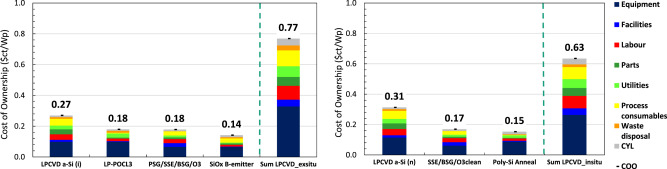
Figure 4. Chief Operating Officer ($ct/Wp) - LPCVD TOPCon in situ (left) and LPCVD TOPCon in situ (right) for each process step unique to the TOPCon concept. Here, it is assumed that the battery conversion efficiency of TOPCon concept on M23 sized wafers is 5.4% to calculate the cost of $ct/Wp. Here, CYL refers to the cost of production loss.
In Figure 5, the total cost of ownership of PERC and TOPCon processes is divided into Wet chemistry, diffusion and annealing, passivation and metallization processes. The Wet chemistry process includes alkaline texture, CEI, glass removal (PSG/BSG), O3 cleaning, and SSE of polysilicon layer. It is observed that the total COO of the Wet chemistry process of the TOPCon route has increased, which is mainly due to the need for additional glass etching, SSE (poly) and cleaning process steps. The diffusion and annealing process includes doping of POCl3 and BBr3a-Si layers, selective laser doping, and high-temperature annealing steps. The COO of the TOPCon route is significantly higher in the diffusion/annealing process here, due to: a) longer duration of the BBr process, 3) comparison between diffusion and POCl, 3) significant decrease in throughput based on the process, and b) the need for additional POCl3 doping process or high-temperature annealing steps for the a-Si layer. The passivation process includes thermal oxidation, LPCVD polycrystalline silicon deposition, PECVD deposition of x/a SiNx stack and a-SiNx: H layer for PECVD AlO. For the TOPCon route, requiring the addition of additional LPCVD deposition steps in PERC typically increases the cost of the passivation process, as shown in LPCVD TOPCon in-situ. However, for LPCVD TOPCon in situ, the process cost is reduced by combining high-temperature annealing and oxidation in a single process step. The cost of metallization includes screen printing of solder pads (Ag) and grids (aluminum and silver/silver aluminum), as well as rapid firing processes. For double-sided p-PERC batteries, the laser contact opening and regeneration process steps are also included in the "metallization" category. TOPCon batteries require significantly higher metallization costs, mainly due to the need to print Ag based grids on both sides to form low contact resistivity contacts. In fact, a significant portion of the process consumables cost in TOPCon battery COO is mainly related to the high silver consumption during the metallization process. Therefore, in order to further reduce the COO of TOPCon batteries, it is necessary to significantly reduce the consumption of silver.
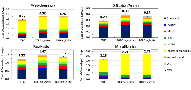
Figure 5. Comparison of the cost of ownership ($ct/Wp) of the double-sided p-PERC and LPCVD TOPon process routes with the cost of each process step of Wet chemistry, diffusion and annealing (diffusion/annealing), passivation and metallization. For double-sided p-PERC solar cells, selective laser doping is grouped with POCl under diffusion/annealing for 3 diffusion processes, while laser contact opening (LCO) and regeneration processes are classified as metallization along with screen printing and firing processes. In the legend, CYL represents the cost of production loss. Here, it is assumed that the battery efficiency of double-sided p-PERC and TOPCon batteries on the M23 wafer size is 0.23% and 5.4%, respectively.
In addition, recent fluctuations in silver prices and the increasing share of the photovoltaic industry in industrial and agricultural use are expected to drive efforts to reduce silver consumption in solar cells. Figure 6 compares the COO of the metallization steps of double-sided p-PERC and TOPCon batteries under various silver reduction conditions. The most optimistic solution to reduce the silver consumption of batteries by 50% of their current value is based on estimates from the International Photovoltaic Roadmap (ITRPV) [42]. Here, we assume that the aluminum consumption formed by the rear grid and the Ag required for the rear label of the PERC battery remain unchanged. The COO of the metallization steps for both battery types has significantly decreased, reducing the consumables costs related to Ag. However, due to the use of Ag on the front and rear contacts of TOPcon batteries, the slope is much higher. It is worth noting that if the future metallization concept allows for a 50% reduction in Ag usage, the metallization cost of TOPCon batteries will be comparable to that of PERC batteries, which may even achieve lower watt peak costs ($/Wp) due to higher battery power.
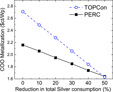
Figure 6. The cost of ownership ($ct/Wp) of the metallization step is estimated to be a percentage reduction in total silver consumption during the industrial screen printing process of the front and rear grids (including busbars and fingers) of the double-sided p-PERC and LPCVD TOPCon process routes. For p-PERC batteries, it is assumed that the total silver consumption is dominated by the front side (the Ag score used for the back label remains unchanged), while the aluminum consumption on the back side remains unchanged in all cases. For p-PERC batteries, laser contact opening (LCO) and regeneration processes, along with screen printing and firing processes, are classified as metallization.
In summary, compared to p-PERC batteries, the TOPCon concept has a significantly higher total cost of ownership at the battery level. Nevertheless, the LPCVD TOPCon in-situ route provides a lower COO between the two studied LPCVD based TOPCon routes.